


Links to raw panoramic photos (CAUTION: files are VERY LARGE, browser might hang):
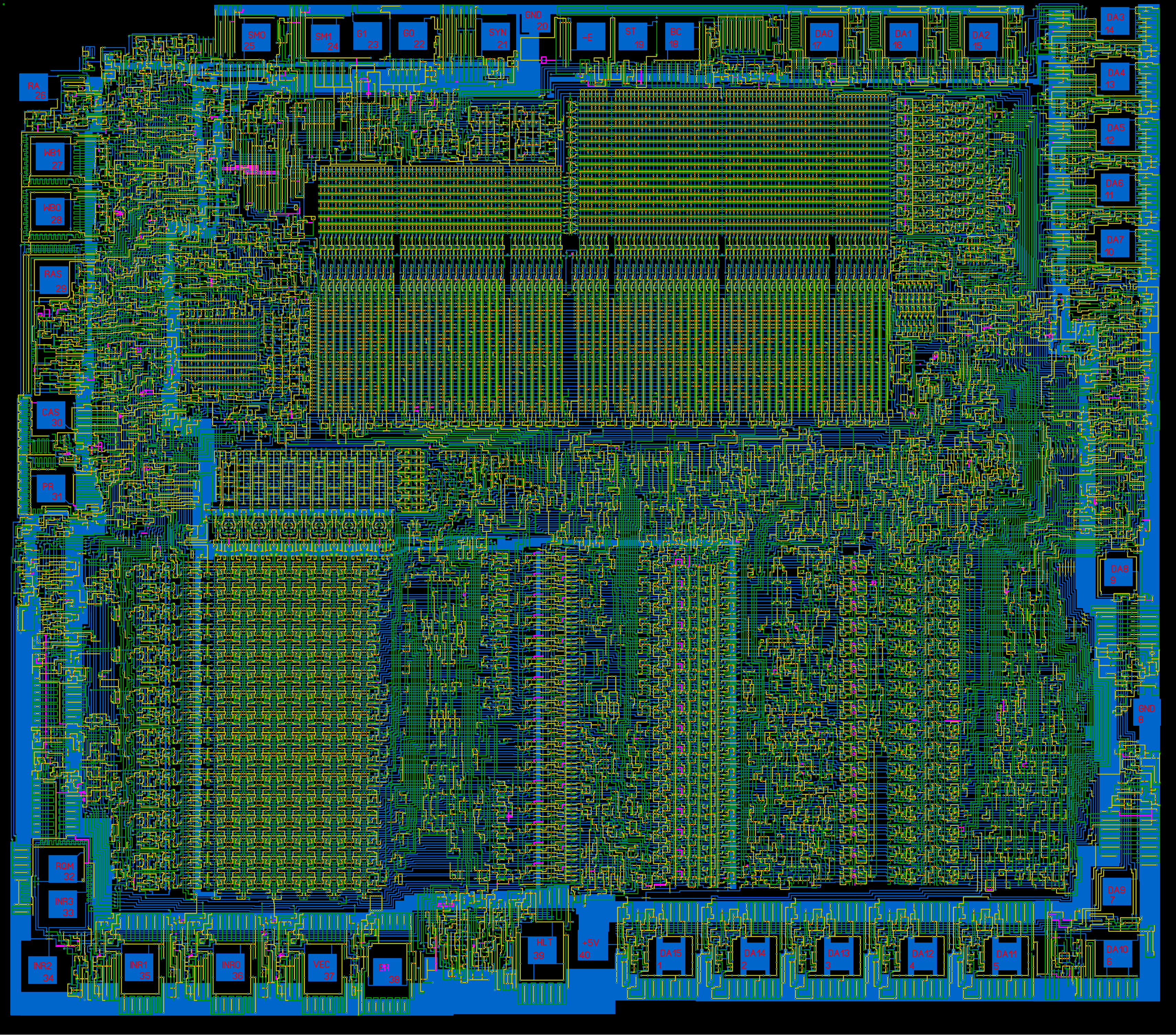
This chapter is about another one DEC PDP-11 processor - T-11, also known as DC310 or DCT11. It was designed in 1981-1982 as single-chip processor and targeted mostly to the embedded systems. "T" stands for "Tiny", it had 40-pin DIP package, multiplexed address/data 16-bit bus, supported directrly dynamic and static memories, dynamic memory refresh, 8/16 bus data widths. The architecture was extremely simplified - there was no refresh timer, no exceptions on bus timeouts, no memory managment, no floating point, and MARK and even EIS instructions was not supported.
"T-11 was the last DEC microprocessor to verify the chip layout manually. For several months, I was part of an army of volunteers that crawled over gigantic Mylar plots of the chip with colored pencils and rulers, tracing lines to make sure the wiring was correct, and measuring gates to make sure the sizing was right. Even with only 12,000 placed transistors, it was a tedious and error-prone process.
After release, the T-11 team drummed up business inside of DEC by holding a design contest. Entrants were encouraged to design a product around T-11; the winning designs would be fabricated. I designed a T-11 based personal computer than fit inside a VT100 terminal and ran RT-11. Although it didn't win the contest, it was interesting enough to be fabricated. This is the only logic design I ever personally did in my career at DEC.
T-11 was the first chip DEC presented at the International Solid State Circuits Conference (ISSCC). At the 1981 show, T-11 ended up sandwiched between Intel's mammoth "mainframe on a chip", the i432, with more than 1 million transistors in the chip set; and HP's Focus chip, with more than 500,000 transistor sites on a single die. Between these two behemoths, the 12,000 transistor T-11 looked, well, tiny. The Semiconductor Group was very discouraged and vowed that its next experience would make a better impression (it did: in 1984, DEC showed both V-11 and MicroVAX).
Ironically, T-11 did far better commercially than either of its ballyhooed session mates. The i432 sank without a trace once its architectural and implementation follies became clear. Focus shipped only a few thousand units. T-11 shipped hundreds of thousands of units and is still running in embedded devices today." - Bob Supnik.
The T-11 was cloned behind the "iron curtain" and produced as 1807BM1 by VFSD ("Voronezh Factory of Semiconductor Devices" - "Воронежский Завод Полупроводниковых Приборов").
The T-11 processor specifics:
- MFPT instruction ("move from processor type", opcode 0000078) supported
- no MARK instruction supported, exception 108 generated
- no odd address trap exception, lower address bit is just ignored in word transactions
- no bus timeout exceptions, no missing memory location failures
- no timer edge-sensitive interrupt request line
- interrupts are requested via "coded priority", either external or internal vector can be used
- all memory writes, except ones to the stack, are preceded with the read of the same location
- extending I/O timing for more than one cycle requires READY signal pulsing
- word transactions with odd addresses work differently on the 8-bit data bus (2 MSBs are read)
- the directory contains HDL-related materials, sources, and sample projects for Quartus and ISE. There are three models: original asynchronous, refactored synchronous and Wishbone compatible
- asynchronous Verilog HDL model is as close as possible to the original gate-level schematics. In practice can be used for modeling purposes only, because processor contains latches (note, it differs from flip-flop), those work in non-reliable fashion on synchronous FPGAs. Nonetheless, this model is included in the package as a demo of the closest possible approximation to the original die. Maybe not synthesizable with some tools, simulation only. The model was fully tested with factory test over all combinations of data bus width (8 or 16 bits) and memory type (static or dynamic).
- synchronous Verilog HDL model, work-in-progress, to be continued
\cad\t11 (pushed to dedicated repo)
Versions updated after the asynchronous model design and verification:
- topology in Sprint Layout format
- topology in PCD-2004 pcb format
- schematics in PCD-2004 sch format